- Samsung Electronics Co, Ltd (OTC:SSNLF) broke ground for a new semiconductor research and development complex in Giheung, Korea, seeking to extend its presence in state-of-the-art semiconductor technology.
- Samsung looks to invest about KRW 20 trillion by 2028 for the complex in an area covering about 109,000 square meters within its Giheung campus.
- The new facility will lead advanced research on next-generation devices and memory and system semiconductors processes, developing innovative new technologies based on a long-term roadmap.
- Samsung aims to overcome the limits of semiconductor scaling and solidify its competitive edge in semiconductor technology.
- The new Giheung R&D facility, together with the R&D line in Hwaseong and the world’s largest semiconductor production complex in Pyeongtaek, will likely elevate the synergy among Samsung’s three main semiconductor complexes in the metropolitan area.
- In the next five years, Samsung aims to invest 450 trillion won ($356 billion) to accelerate growth in semiconductors, biopharma, and other next-gen technologies. The investments will likely create 1.07 million jobs.
- Samsung is also one of the frontrunners for the U.S. Chips Act involving a $52 billion federal program to boost domestic chipmaking capabilities.
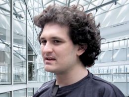
Sam Bankman-Fried, Founder Of FTX, Appeals Fraud Conviction And 25-Year Sentence
Sam Bankman-Fried, the founder of cryptocurrency exchange FTX, has lodged an appeal against his fraud conviction and 25-year prison sentence, which he received for his involvement in one of the largest financial frauds in American history.